
My name is Raul Perez, and I am the CEO at Custom Silicon. I have 20 years of experience in the electronics industry, specializing in chip design and system electronics.
I started my career at Texas Instruments, designing different types of custom silicon for several major companies. I then transitioned into the system electronics industry, working for companies like Apple where I ramped over 20 custom chips for Microsoft HoloLens, dual devices, and Snap Spectacles.
What is custom silicon?
Custom silicon is used by a system electronics company when they decide they no longer want to base their electronics on off-the-shelf, available components in the market.
When buying analog parts, fats, and diodes to fill your board, you’re usually left with lots of parts you don’t really need. These components are part of a chipset because they're made for a broad market.
As such, you decide that you want to have a more compact and custom design. You want to put all the useless parts laying around the board in a nice package to save on costs.
You then decide that you're going to make your own chip. However, a lot of the companies that develop their own custom silicon don't go 100% custom or 100% catalog, they'll have a mixture of both.
Usually, you'll be in a position to focus solely on what will differentiate the product. For people who make phones, that tends to be the processor. They will take over the processor design and build a substantial semiconductor team to start making their own processor. But that doesn't mean they’re going to make their own power management chip or other chips that go around it.
That's when you partner with a semiconductor supplier.
When you partner with a chip supplier to make a custom silicon part, you have to develop an engagement model and a process on how to work with them. You also have to carefully select the ideal people that will do this type of work for you. That's where custom silicon management comes into play.
The benefits of custom silicon
People make custom silicon decisions based on their system and industry. In consumer electronics, it's a pretty clear ROI. If your volume is high enough, the custom silicon will pay for itself and you’ll make your money back in a few months. Both your costs and your footprint size will also decrease to 50% of what they would have been had you been doing discrete components.
Another important benefit of custom silicon is that your product cannot simply be reverse-engineered. A lot of companies can extract firmware and schematics to find out what you have in your product. They can carry out all sorts of malicious activity or clone your product.
When you go down the custom silicon route, you can obscure your IP address. Companies won’t be able to poke around and probe the signals to try and figure out what you're doing because all the information they need is hidden inside the silicon. You can enhance your security and implement your IP just the way you want.
The challenges of custom silicon
Many people are scared of adopting custom silicon, and rightfully so; if your entire system depends on that silicon working and it fails, your schedule will be directly impacted.
Silicon management provides a way of mitigating the risk that you incur. This way, you can get all the goodness you want from custom silicon without entering some freefall schedule issue where you don't know when you're going to be able to build, and every time you turn silicon you have a month and a half to two months' wait.
Luckily, the semiconductor industry is pretty mature and the tools are fairly advanced. This is because the mass sets became so expensive for the advanced nodes that there had to be a big investment. As such, the silicon industry is lightyears ahead in terms of CAD and methodologies on how to do verification before tape out.
Verification is an area where innovation is happening and needs to happen. But you need to be able to predictably mitigate your risks to be able to develop custom silicon so you can ramp your system.
The main goal is to avoid serializing things. Some that buy chipsets have to wait for them to be ready to begin doing system development. Chipset companies might work with the big players as they are developing the chipset, but generally, they won’t do this.
If you develop your own chip, you're going to be a generation ahead of everybody else. However, you need to know what you're doing and have the right people working in the system electronics company.
Following the custom silicon schedule
Below is a mock-up schedule from the Custom Silicon website, which I will explain in detail.
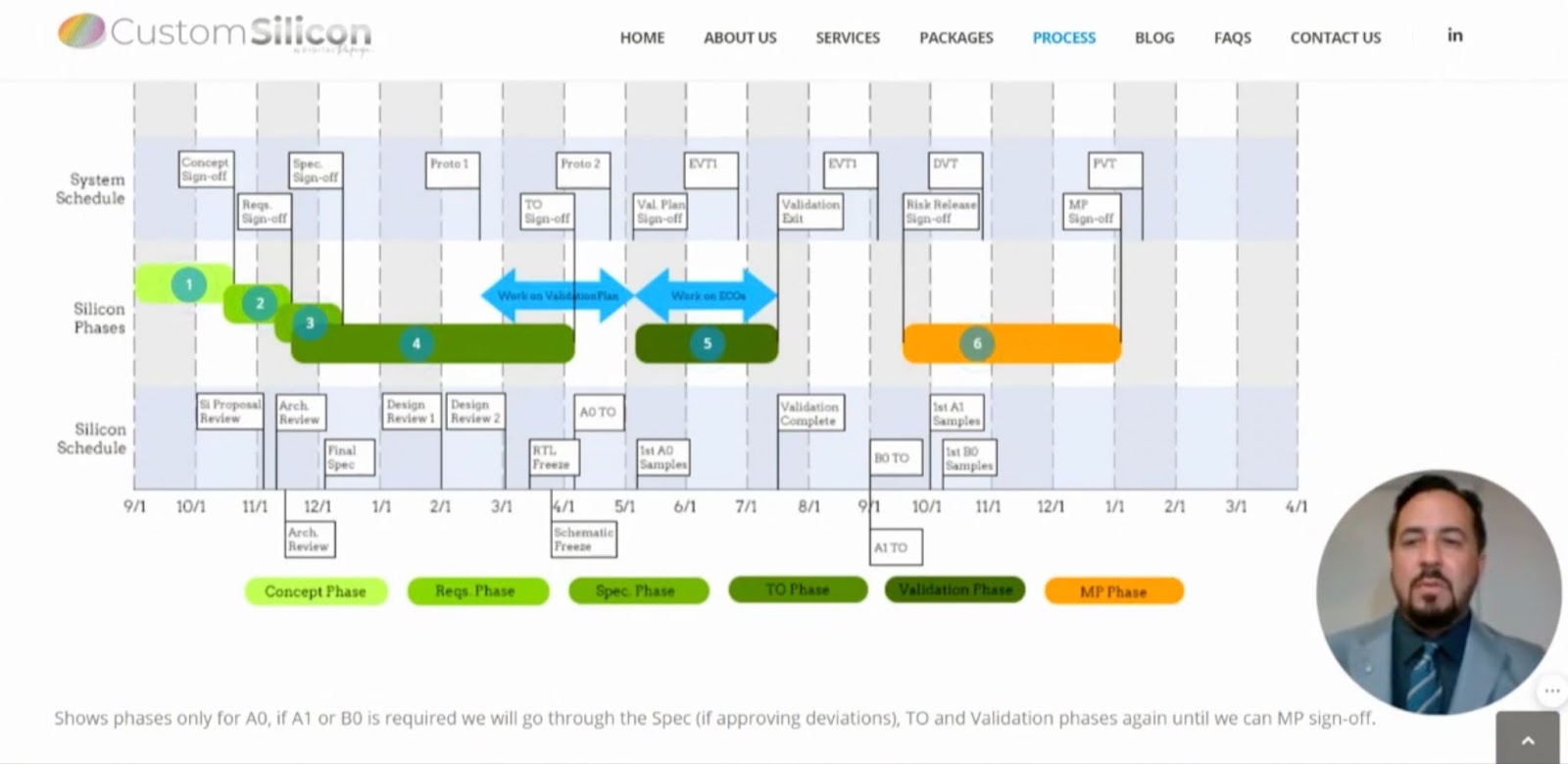
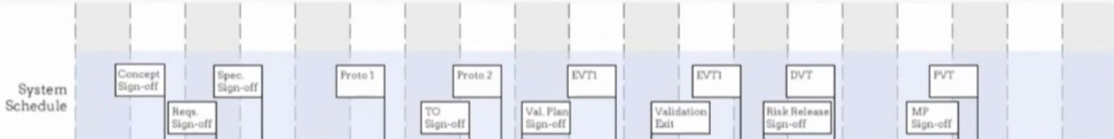
System schedule
This part of the schedule is where you’ll have some builds, and as you're trying to bring up your system, the amount of protos you have will depend on how mature your previous product is, or how different the new derivative product is. Or if you have a brand new product that doesn’t have a previous generation, you might have more proto builds.
When you get to EVT, you'll try out your more stable candidates. Then you'll get to DVT, which is the final engineering build where you try to prove your shipping candidate to see how it does. By this time, you've usually downselected to a single design. PVT is when you ramp; it's your DVT design, but in a much larger quantity.
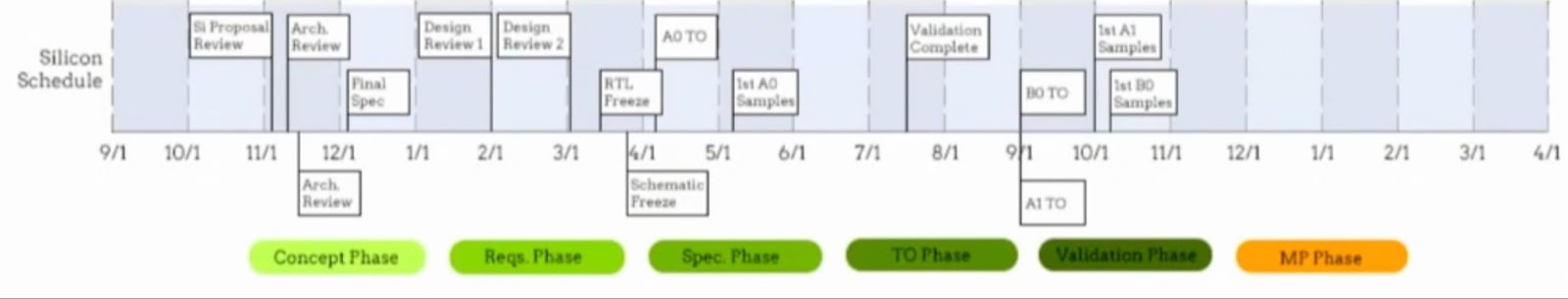
Silicon schedule
As you're doing custom silicon, you'll have a silicon proposal review where you search for and talk to suppliers, and perhaps carry out an architectural review afterward. You'll have some spec, draft spec, final spec, and multiple design reviews before tape out.
There’s also RTL freeze, schematic freeze, and then taping out your first silicon and getting your first samples. You'll have to go through a validation process, another tape out, and then you'll get another sample back.
Normally, you'll plan for when the silicon doesn't have a lot of new things in it. You're not doing invention or R&D in this chip, but you're making modifications to existing unknown IP. You'll usually be able to get it done in one base spin and one metal, but you may have to do two base spins depending on what's broken in your first turn.
Typically, EVT has to have your first rev of the silicon, then you want to have it at proto. You always want to try and have it at the earliest point possible, but it depends on what silicon this is. If your silicon is actually the processor, you're most likely the one driving the system schedule and therefore, the one that's driving when EVT happens.
If you have a previous system, you might be able to use some of the previous silicon to start building up your new system. For proto one, it's mostly the same old system with the same old drivers and software. As you get a new module or some chip comes in, you're writing your new driver, combining it with the old stuff, and the product is that bit closer to what you want.
By the time you get to EVT, you should have all the first modules, chips, and other components of your new system in place. You’ll then move on to writing drivers and software as the start of your software development.
You might have multiple EVTs depending on how many software features you have and how many bugs have occurred. It could also be that you have multiple DVTs; you might think that the design is ready to ship but you find some problems and have to plan a second DVT.
DVT is usually the last point where you would input anything new, but ideally, your chip has to be ready before the DVT build.
The silicon phases
The custom silicon itself has a number of phases: concept, requirements, spec, tape out/design, and validation.

You might have to risk releasing some material as suppliers usually require three to four months of ramp time. If you're on the one-year cycle, by the time you want to have your PVT ramp there's usually not enough time between DVT and PVT. Therefore, you'll have to risk releasing material before DVT exit data is available. This data is what you need to be able to sign off the chips.
You’ll have to approve buying material and kicking off wafers and packages based on incomplete validation results from the system. Therefore, you'll have to assign some risk level to each thing and then be willing to potentially scrap that material, which could cost millions of dollars.
Every silicon phase is signed off by the stakeholders. These are all the cross-functional team members that are needed to make the chip happen and integrate it into the system. So when you're working with a supplier, you need to identify which people at the system electronics company are the stakeholders for each team.
The concept phase
In this phase, the system engineers will be testing ideas and multiple prototypes. You’ll go to the suppliers that you're already working with to tell them what you're doing and perhaps indirectly ask them what kind of technology they’d have or explain what you would like to have in the chip.
Everybody should strive to have a good working relationship when developing silicon with their partners, so it’s important to share as much information with them as possible.
The requirements phase
In this phase, you'll get more input from the PRD for the system itself and your requirements are more driven by the system PRD. You’ll also continue to have conversations with suppliers.
At the end of the requirements, you’ll want to narrow your supplier options down to two. You'll also hopefully have had the opportunity to get a proposal from the two companies you think are the best for your project before signing off.
When you do a silicon proposal review, looking at some PowerPoint slides that a marketing and sales guy have put together is not enough. You need to conduct other verification methodology reviews.
You need to know exactly what tools the company uses and how they do verification for the type of chip you want. You also need to see test benches and some sample test codes. Whenever there's some IP that they're going to be using, you want to know if it’s a pre-verified IP or their own.
Having people on your side in the system electronics company with expertise in all these different areas is a big advantage because you’ll hopefully end up with a partner that helps you develop silicon for your system and it's not going to be a one-shot thing, it's going to be a generation after generation thing.
The next generation is going to be a delta for you, which means less risk and fewer engineering man-hours. And you’ll keep your custom solution that's difficult to reverse engineer.
Before you close requirements, you'll have done a review and understood who the suppliers are, the IP they have, what the delta is, and what the risks are from each proposal. You’ll also know the toolsets they're using, the methodology, and the talent they have, and have talked to the verification and designer guys.

The spec sign-off phase
When you enter the spec sign-off phase, the supplier should give you a draft spec of what the chip is going to do.
This spec will be negotiated for a few weeks, and at the end of the spec sign-off, you will receive a data sheet from the supplier detailing what they can do for you. At this point, your engineers must look at it and decide if it’s good enough to meet your requirements.
You have to look at how each parameter is going to be guaranteed. Is it guaranteed by design or by bench evaluation? Is it all ATE tested? These things could be agreed upon later, but the later you do it, the less chance you'll have to get what you want.
The design phase
Once you do the spec sign-off, the chip is likely already in the process of being designed. At this point, you can go back and forth with the supplier in case they find any design requirements they’re not able to meet.
You’ll want to fly out two design reviews to the chip design company before the first tape out, and in these reviews, you're going to be looking at the verification plan. You’ve checked the verification methodology requirements, but now you want to see what the actual plan is. What are they testing? What do the test benches look like? How much is the transistor level? What are they covering in regards to the DV?
You want to understand precisely what they're going to be testing, but also that they're testing use cases that you as a system designer know are important. You can give them ideas about ways in which you’re planning to use the chip. Give them as much information as you can so that they can create a verification plan that is as close as possible to what you will use for your system.
You should discuss the two design reviews at the chip design company site so you have as much access to their engineers as possible.
Once you've agreed on the verification plan that's going to be executed, you’ll get the verification collateral back so that you can review it and make sure that everything looks good. Then the chip will get taped out.
The validation phase
Once the chip is taped out you'll be waiting to get the samples back. During that time, you should have a validation plan, review, and sign-off so that everybody is aware of what the supplier is going to be validating on the bench and ATE.
Try to use the supplier’s resources as much as possible to check the chip and produce some validation reports so that the system engineers can focus more time on using them as a reference for their debugging at the factory, or as they do their system integration.
Now that you've got your first sample, you’ll start doing your validation exit. You'll probably intercept your first possible build and then get some feedback from the build and the validation of the chip itself, which will fit into your next tape out. You'll then decide whether it's a full base or metal only.
That tape out will give you your next sample. if you're going really fast, it's aligned with your DVT and is the last build where you’re able to input something new. Hopefully, you've been very judicious, because if you’ve got silicon going into DVT, you have to be careful what you're going to change.
Once you get into DVT, you need to understand what your OTP settings are; if your chips are getting programmed with OTP when you do the risk release, you'll have to know what this OTP is so that the assembly and test can be finished.
If your design is ready at risk release sign-off and you're getting ready to go to PVT, both you and the supplier will do the validation during this stage. DVT exit data will be available and then so will the final validation data from the supplier.
They're doing everything that a normal chip supplier would do; they have an ATE program, they're offshoring the program, they're doing their characterization review, and they're releasing the datasheet for production.
Nothing that we do in silicon management should create a big burden on the chip suppliers besides the reviews.